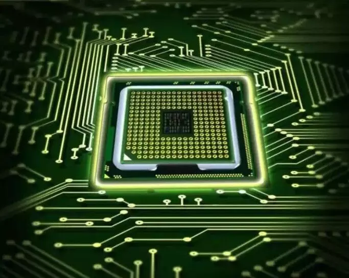
What is HDI Printed Circuit Board? Guide to High Density Interconnect PCB

In today’s rapidly evolving electronics industry, devices are becoming smaller, faster, and more complex. This trend has created a demand for advanced printed circuit boards (PCBs) capable of handling high component density and performance. Among the most popular solutions is the HDI printed circuit board, also known as High Density Interconnect PCB. But what exactly is an HDI PCB, and why has it become essential for modern electronics? This article provides a comprehensive guide on this technology and its benefits.
Understanding HDI Printed Circuit Boards
HDI printed circuit boards (PCBs) are designed to provide higher wiring density per unit area than traditional PCBs. The term “HDI” stands for High Density Interconnect, which refers to the capability of the board to interconnect a large number of components in a small footprint. Unlike conventional PCBs that rely primarily on through-hole connections, HDI boards employ advanced techniques such as microvias, blind vias, and buried vias to optimize space utilization and maintain high electrical performance.
The main goal of HDI PCBs is to maximize the number of connections between layers while minimizing the size of the board. This makes them ideal for devices that require high-speed signal transmission, compact form factors, and advanced functionality.
Key Features of HDI Printed Circuit Boards
- Microvias – Microvias are tiny holes that connect different layers of the PCB. They are smaller than traditional vias, which allows for more complex and dense interconnections. Microvias are often laser-drilled, ensuring precision and reliability.
- Blind and Buried Vias – Blind vias connect external layers to internal layers without passing through the entire board, while buried vias connect internal layers only. These features reduce the amount of space taken up by vias, allowing for more routing area for circuits.
- High Layer Count – HDI PCBs can support multiple layers, often exceeding six or eight layers in advanced designs. This capability supports more complex circuitry while keeping the overall PCB size compact.
- Fine Line Technology – HDI boards use finer traces and spacing between lines, enabling higher density routing and supporting high-frequency applications.
- Enhanced Performance – The reduced signal path length and controlled impedance of HDI PCBs improve signal integrity, reduce electromagnetic interference (EMI), and support faster data transmission rates.
Advantages of HDI Printed Circuit Boards
HDI printed circuit boards offer several benefits over traditional PCBs, making them ideal for modern electronic devices:
- Compact Size: The use of microvias and fine lines allows HDI PCBs to pack more components into a smaller area, which is crucial for smartphones, tablets, and wearables.
- High-Speed Performance: HDI PCBs support high-frequency signals with minimal signal loss, making them suitable for 5G, IoT, and high-performance computing.
- Reliability: By reducing via length and optimizing interconnections, HDI PCBs improve thermal and mechanical reliability, which is essential for mission-critical devices.
- Flexibility in Design: Designers can implement complex circuitry without significantly increasing the PCB size, allowing for more innovative and compact products.
- Better Signal Integrity: Shorter electrical paths reduce cross-talk and impedance mismatch, improving overall signal quality.
Applications of HDI Printed Circuit Boards
The hdi printed circuit board is widely used in modern electronics where compact size and high performance are essential. Some common applications include:
- Smartphones and Tablets – HDI PCBs allow manufacturers to pack multiple layers of circuitry into thin and compact devices, supporting features like high-speed processors, advanced cameras, and wireless connectivity.
- Wearable Devices – Devices such as smartwatches and fitness trackers rely on HDI PCBs to integrate complex electronics into a small, lightweight form factor.
- Automotive Electronics – Modern vehicles utilize HDI PCBs in applications like advanced driver-assistance systems (ADAS), infotainment systems, and electric vehicle power electronics.
- Medical Devices – Portable medical instruments and diagnostic tools benefit from the miniaturization and reliability offered by HDI PCBs.
- Aerospace and Defense – HDI PCBs are used in avionics and military applications where space constraints and high reliability are critical.
Manufacturing Considerations for HDI PCBs
Producing HDI printed circuit boards requires advanced manufacturing processes. Some important considerations include:
- Precision Drilling – Microvias are laser-drilled with high accuracy to maintain proper alignment and electrical connection.
- Layer Registration – As HDI boards often have multiple layers, precise alignment is essential to prevent defects.
- Material Selection – High-quality substrates with stable dielectric properties are used to ensure signal integrity and thermal performance.
- Advanced Assembly Techniques – Due to high component density, assembly often requires surface-mount technology (SMT) and automated placement machines.
Future of HDI Printed Circuit Boards
As electronics continue to evolve, the demand for smaller, faster, and more reliable devices will increase. The HDI printed circuit board is at the forefront of this evolution, enabling innovative designs in consumer electronics, medical devices, automotive systems, and beyond. Advances in microvia technology, fine line routing, and materials science will continue to push the boundaries of what HDI PCBs can achieve.
Conclusion
The HDI printed circuit board is a game-changer in modern electronics. By combining compact design, high-speed performance, and reliability, HDI PCBs enable manufacturers to create sophisticated devices that meet the demands of today’s technology-driven world. Understanding what is HDI printed circuit board and how it works is crucial for engineers, designers, and technology enthusiasts who want to stay ahead in the rapidly changing electronics landscape.
For anyone exploring advanced PCB design, this guide to high density interconnect PCB serves as a comprehensive reference to understand the technology, benefits, and applications of HDI boards.
Woman injured in stabbing attack in Tokyo, suspect at large
Bengal cop booked for murder over mysterious death of woman home guard, SIT to probe case
Staffer recalls horror of 7-kg gold robbery by armed gang in Karnataka’s Hunsur
25-Year-Old Airline Cabin Crew Member Dies At Gurugram Party; Police Begin Investigation


